
What are the process of PCB manufacturing? PCB are used in almost all electronic products, ranging from watches and earphones to military and aerospace applications. Although they are extensively used, utmost people don’t know how PCBs are produced. Let us learn something about soldering and the PCB manufacturing process!
The appearance of the PCB is shown in the below:
Single-sided panel production: Make the designed circuit into a negative, then transfer the circuit on the negative to a thin layer of copper foil, and dissolve the unnecessary copper foil with chemicals to get the circuit we need .
Drilling and electroplating: If you want to make a double-sided or multi-layer board, you must first make a via (Via), a buried via hole (Buried via hole), a blind via hole (Blind via hole), generally you can use mechanical drill (Mechanical drill) Drill directly with a drill bit, the minimum size of the hole is 8mil (about 0.2mm); you can also use laser drilling (Laser drill) to penetrate the plastic plate with laser light, the minimum size of the hole can reach below 4mil (about 0.1mm) , to make copper wires thinner and denser, we call it HDI process (High Density Interconnection)
Multi-layer printed circuit board bonding: the prepared double-sided boards are bonded to form a multi-layer board. When bonding, an insulating layer (plastic material) must be added between the layers. If there are perforations (Via) that penetrate several layers, then each layer The above steps must be repeated. The lines on the front and back surfaces of the multilayer board are usually made after the multilayer board is bonded.
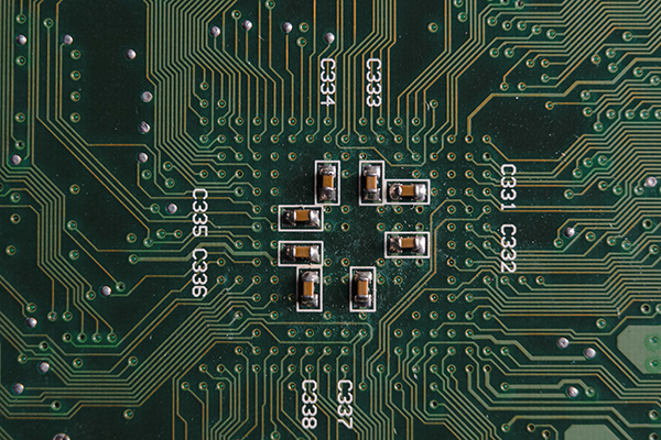
Protection and surface treatment: The green or brown on the printed circuit board is the color of the solder mask (Solder mask), which is an insulating protective layer that can protect the copper wires from oxidation. Layer screen printing surface (Silk screen), on which text and symbols will be printed to mark the name and position of each integrated circuit (IC) and other electronic components, the screen printing surface is also called icon surface (Legend), if this If the printed circuit board has gold fingers, then the circuit of the gold fingers will be electroplated at the end.
Circuit test: It is used to test whether there is a short circuit or an open circuit on the printed circuit board. Generally, the optical method can be used to scan the board with infrared light to find the defects of each layer, and to detect whether there is an incorrect gap between the wires; it can also be used Electronic testing uses a flying probe (Flying probe) to check the connection of all copper wires to determine whether there is a short circuit or an open circuit.
In short, the PCB manufacturing process is very complicated. If you want to know more about it, please pay attention to the AiXun official website.
 WhatsApp